Specifications
Physical
| RockBLOCK 9704 ANT | |
|---|---|
| Size | 59 × 36.5 × 7.7 mm |
| Weight | <10g (excluding antenna) |
| Form Factor | 3mm mounting holes, positioned diagonally across board corners |
| Antenna | External PNT antenna required. |

CAD data
CURRENT VERSION - CAD data STEP-RockBLOCK APNT Rev 1e - MMCX version
PREVIOUS VERSION - CAD data STEP-RockBLOCK APNT Rev 1d - U.FL version
Hardware (Revision 1E upwards)
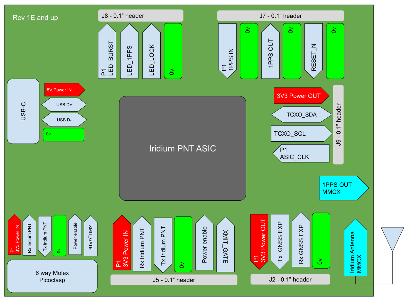
J1 PicoClasp and J5 0.1" pitch header - Main interface
| Pin | Label | Description | Type | Direction |
|---|---|---|---|---|
| 1 | VDC | 3.3V | Power | Power |
| 2 | ASIC_RX | ASIC Rx | 3V3 logic via level shift | IN |
| 3 | ASIC_TX | ASIC Tx | 3V3 logic via level shift | OUT |
| 4 | GND | Power Ground | GND | Power |
| 5 | PWR_EN | Drive high to enable ASIC power. | 3V3 Logic | IN |
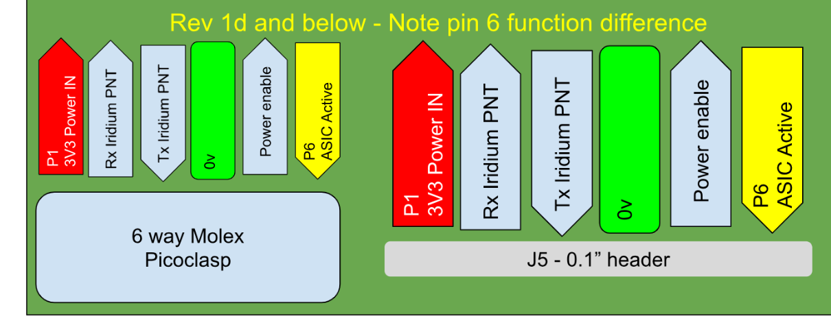
| 6 | XMIT_GATE (Previously ASIC Active - function changed from rev 1E) | Drive high to supress onboard LNA | 3V3 Logic | IN |
J2 0.1" pitch header - GNSS Add on
| Pin | Label | Description | Type | Direction |
|---|---|---|---|---|
| 1 | 3V3 out | 3.3V via ferrite BLM18KG331SZ1D | Power | Power out |
| 2 | GNSS_TX | External GNSS Tx | 3V3 logic via level shift | OUT |
| 3 | GNSS_RX | External GNSS Rx | 3V3 logic via level shift | IN |
| 4 | GND | Ground | GND | GND |
J7 0.1" pitch header - ASIC Control
| Pin | Label | Description | Type | Direction |
|---|---|---|---|---|
| 1 | 1PPS_IN | Input from external PPS source | 1V8 Logic | IN |
| 2 | GND | Ground | GND | GND |
| 3 | 1PPS_OUT | Output from internal PPS source | 1V8 logic | OUT |
| 4 | GND | Ground | GND | GND |
| 5 | RESET_N | Pull low to reset the PNT ASIC (Internal 10k pull up) | 1V8 Logic | IN |
| 6 | GND | Ground | GND | GND |
J8 0.1" pitch header - LED Out
| Pin | Label | Description | Type | Direction |
|---|---|---|---|---|
| 1 | LED_BURST | Signal LED indicator for burst detection | 3V3 logic via level shift | OUT |
| 2 | LED_PPS | LED indicator for 1PPS | 3V3 logic via level shift | OUT |
| 3 | LED_LOCK | LED indicator for lock state | 3V3 logic via level shift | OUT |
| 4 | GND | Ground | GND | GND |
J9 0.1" pitch header - I2C interface
| Pin | Label | Description | Type | Direction |
|---|---|---|---|---|
| 1 | ASIC_CLK | Alternate clock input for ASIC - Requires fitment of 0R link for R65 and removal of R41 (R60 load may need to be adjusted) | 1V8 Logic | IN |
| 2 | TCXD_SCL | I2C SCL | 3V3 logic via level shift | IN |
| 3 | TCXD_SDA | I2C SDA | 3V3 logic via level shift | - |
| 4 | 3V3 | Power out - direct from internal 3V3 rail. Under PWR_EN control | Power | Power out |
Environmental
| Ingress | N/A |
| Operating Temperature | -20°C to +70°C |
Regulatory Compliance
- Iridium Certification in progress.
Electrical & Power
| Voltage | 5 V via USB-C or 3.3 V via Molex PicoClasp 5015680607 |
| Power consumption (Peak) | <1.2W |
| Power consumption (Idle) | ~0.95W |
Communication Interfaces
| APNT antenna | U.FL connector |
| 1PPS Out (Timing) | U.FL connector |
| Serial | TTL UART connection (default: 115200baud) |
| USB-C | USB-Serial bridge (default: 115200baud) |
| Digital GPIO | See diagram below. |
Pin function (Revision 1E upwards)
Pin function difference (Revision 1D and lower)
danger
These documents are intended to provide early access information to interested parties during the development process. Whilst we strive to maintain accuracy, any part of the specification or design of these products may change without notice.
These documents were last reviewed for accuracy on 5 Nov 2026.